Printed ceramic gas rings target advanced semiconductor processing
A 500 mm alumina component supports deposition and etching within the same process chamber.
What happened
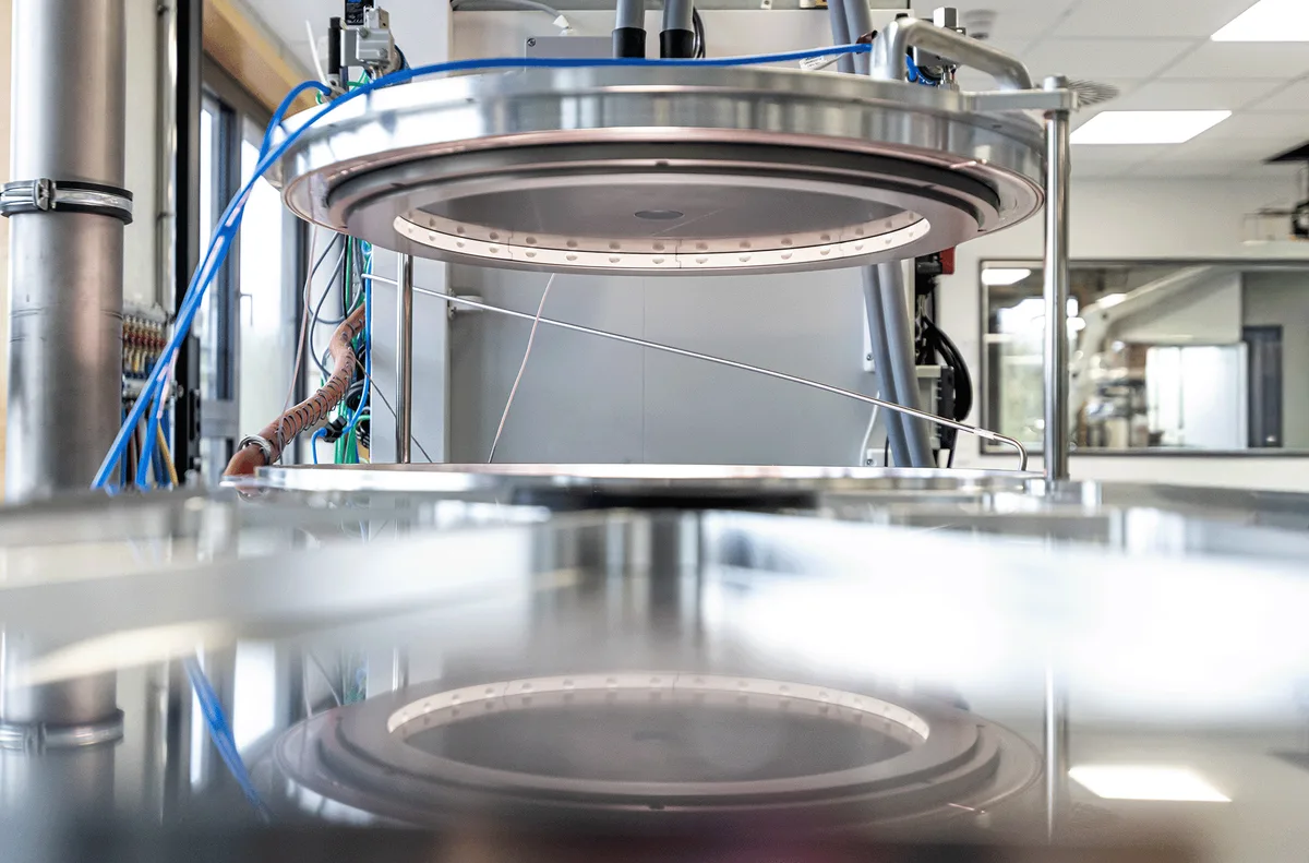
Plasway-Technologies, Alumina Systems and Lithoz developed a dual-channel alumina gas-distribution ring for semiconductor equipment. Lithoz’s June report describes a component measuring 500 mm.
The ring supports Plasway’s FAST Atomic Layering Process platform, combining plasma-enhanced atomic-layer deposition and atomic-layer etching in one chamber. The design aims to distribute process gases uniformly across large substrates.
This application places ceramic additive manufacturing inside the equipment used to make chips. It illustrates the value of complex internal passages, rather than suggesting that the semiconductor chips themselves are 3D printed.
Read the sources
Primary-source reporting; this is not a hands-on review. Sources checked Oct 25, 2026.