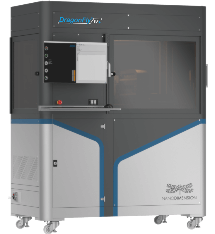
 Inkjet material depositionManufacturer image: Nano Dimension
Nano Dimension DragonFly IV+
Additive electronics system co-depositing conductive silver and dielectric inks.
Source reviews: 2026-10-16.
Specifications are reported claims, not independent test results.
The details that matter.
Published specifications for this model. Follow a field's source for its configuration and measurement conditions; older fields refer to the profile's reference list.
| Introduction year | Not verified |
|---|---|
| Model family | DragonFly |
| Process | Inkjet material deposition |
| Build envelope (X × Y × Z) | 160 × 160 × 1.7 mm |
| Nominal box volume | 0.04 L · calculated from the envelope |
| Enclosure | Not verified |
| Materials cited in this profile | Conductive silver nanoparticle ink, Dielectric ink |
| Manufacturer listing status | Official documentation available; current order availability not confirmed |
| Regional stock and price | Check the manufacturer |
| Market grouping | Industrial · editorial grouping |
Technical specifications
| XY Resolution (µm) | 18 Reported X/Y deposition resolution; not electrical trace spacing or dimensional accuracy. |
|---|---|
| Z Resolution (µm) | 10 Reported Z resolution; the page separately lists 5.4 µm dielectric and 1.3 µm conductive layer minima. |
| Machine dimensions (mm) | 1400 × 800 × 1800 |
| Machine weight (kg) | 520 |
| Power Supply | 230 VAC, 20 A, 50–60 Hz; UPS required |
| Connectivity | Ethernet TCP/IP 10/100/1000 |
| Operating Temperature (°C) | 18–25 |
| Operating Humidity | Above 35%, non-condensing |
| Printhead Count | 2 |
| Deposition | Piezoelectric drop-on-demand inkjet |
| Minimum Trace Width (µm) | 100 |
| Minimum Trace Spacing (µm) | 150 |
| Minimum Via (µm) | 200 |
| Minimum BGA Pitch (µm) | 400 |
| Software | FLIGHT HUB |
Conductive and dielectric printing
DragonFly IV+ deposits silver nanoparticle and dielectric inks through separate printheads to construct multilayer electronic structures. Its workflow supports substrate geometry, conductive traces and passive elements using FLIGHT design and preparation tools.
Electrical geometry and test conditions
The current IV+ table lists a 160 × 160 × 1.7 mm build volume, 100 µm minimum traces and 150 µm spacing. Raster resolution is separate from trace design rules. Electrical properties are typical controlled-test values and depend on geometry, orientation, settings and environment; they should not be treated as universal circuit-design limits.
Explore the model family.
An exact introduction year has not been established in the reviewed sources.
Family: DragonFly · Listing status only
Explore Nano Dimension through the generationsRead this with the specifications
The current page heading and specification table identify DragonFly IV+, although the URL retains dragonfly-iv. This profile uses the IV+ table and its 1.7 mm maximum board thickness; earlier IV claims of 3 mm height are not merged into it. Deposition resolution is distinct from trace width and spacing.
A larger nominal envelope does not establish better print quality. Fit depends on the configuration, usable area, supports, and orientation.